
3D Printing Method Fabricates Complex Metal Plastic Composite Structures
Researchers from Japan and Singapore have developed a new 3D printing technique to create precise metal patterns on the surfaces of 3D plastic structures to target next generation electronics.


Researchers at Waseda University of Japan and Nanyang Technological University of Singapore recently published a paper describing what they call multimaterial digital light processing 3D printing (MM-DLP3DP) — a process that can fabricate metal plastic composite structures with arbitrarily complex shapes. Waseda’s Shinjiro Umezu and Kewei Song along with Hirotaka Sato from Nanyang published the study in ACS Applied Materials & Interfaces.
The researchers noted that existing technology can manufacture 3D circuits, but stacking flat circuits is still an active area of research. Current technologies for fabricating such structures tend to be expensive with a high degree of complexity, long production cycles and low-design flexibility. The multi-step MM-DLP3DP process begins with the preparation of the active precursors, which can be converted into the desired chemical after 3D printing since these chemical aren’t printable.


To achieve this, palladium ions are added to light-cured resins to prepare the active precursors. This allows electroless plating (ELP) wherein an auto-catalytic reduction of metal ions in an aqueous solution forms a metal coating. Next, the MM-DL3DP apparatus is used to fabricate microstructures containing nested regions of resin or the active precursor. In the final step, these materials are directly plated, and 3D metal patterns are added to them using ELP.
Additive Manufacturing 101
New to additive? Learn about materials, processes, trends, workflow and more on the New to AM? site.
Such 3D metal–plastic composite structures have widespread potential applicability in smart electronics, micro/nanosensing, internet-of-things (IoT) devices, and even quantum computing, according to the researchers. 3D printing these structures gives the devices they’re put into a higher degree of design freedom, with the possibility more complex features and geometry, as well as increasingly smaller sizes. They have not been widely adopted, however, because the current methods to fabricate such parts are expensive and complicated.
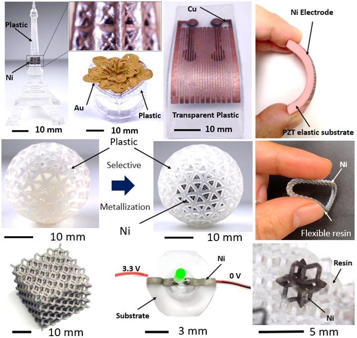
To demonstrate the manufacturing capabilities of the MM-DLP3DP process, the research team created parts with complex structures including multimaterial nesting layers and microporous and tiny hollow structures — the smallest of which was 40 μm in size. The metal patterns on these parts were very specific and could be precisely controlled. The team also manufactured 3D circuit boards with complex metal topologies, like an LED stereo circuit with nickel and a double-sided 3D circuit with copper.
In addition to creating highly specific metal patterns, the paper notes that the process results in higher quality metal coatings, both of which can contribute to highly integrated and customizable 3D microelectronics.
The Researchers believe this advance represents a breakthrough technology for the manufacturing of circuits, with potential application 3D electronics, metamaterials, flexible wearable devices and metal hollow electrodes.
The researchers believe this advance represents a breakthrough technology for the manufacturing of circuits, with potential applications in 3D electronics, metamaterials, flexible wearable devices and metal hollow electrodes.
Photo Credit: Waseda University
Related Content
-
High-Flow PEI ‘Captures’ Burn-In Test Socket Manufacturer
S. Korea’s Sensata is one of the first BiTS makers to adopt SABIC’s new Superflow Ultem.
-
Artificial Intelligence Enables Smarter Sourcing
Westfall Technik has adopted Arkestro’s predictive procurement software to wring savings and more reliable deliveries from a historically challenging supply chain.
-
Record Reshoring Rates in 2022
Reshoring and foreign direct investment (FDI) in the third quarter marked their highest ever level, eclipsing the previous record set in the second quarter of 2022.


